Choose a Memory IC by defining what the system must store and how the host must access it. Then verify the required density and organization, interface and timing, supply and I/O voltage, and exact package. These four specifications narrow the field, but they do not prove that one device can replace another.
The final choice also depends on volatility, write pattern, endurance, retention, temperature, power, controller support, firmware behavior, qualification, and product lifecycle. For an existing design, the current manufacturer datasheet, ordering table, schematic, PCB footprint, and software requirements should govern the comparison.
This Memory IC selection guide gives engineering and procurement teams one review sequence. It also turns the approved requirement into an RFQ that a supplier can quote without guessing the part, package, grade, or acceptance conditions.
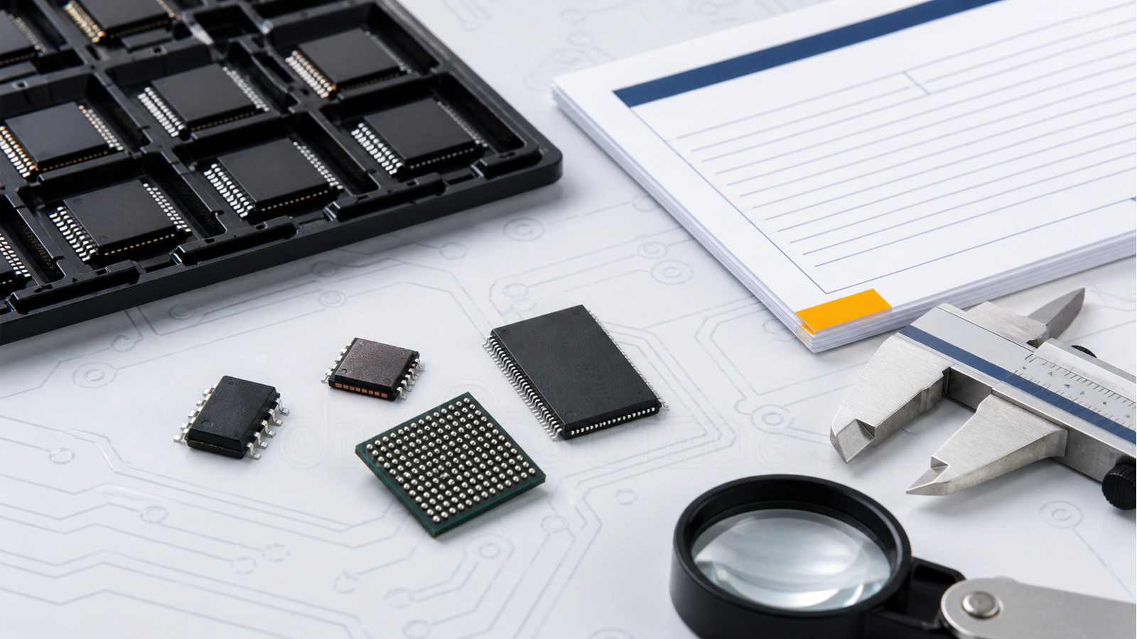
Compare the memory type, density, interface, voltage, and exact package before approving a part for sourcing.
Quick answer: how to choose a Memory IC
Use this sequence to choose a Memory IC:
Define the data. Decide whether it must survive power loss, how often it changes, how quickly it must be available, and whether the system needs random access, code execution, buffering, or bulk storage.
Choose the memory family. Compare EEPROM, NOR flash, NAND or managed NAND, SRAM, DRAM or LPDRAM, and specialist nonvolatile RAM against that data behavior.
Calculate usable density. Include payload, metadata, logs, update or rollback space, growth, and any device-level reserved capacity. Confirm bits versus bytes and the memory organization.
Match the interface. Verify the host controller, bus width, protocol, command set, clock or access timing, boot support, topology, and software impact.
Check every voltage domain. Compare operating ranges, I/O levels, sequencing, reset behavior, power modes, and absolute maximum ratings.
Confirm the exact package. Match the ordering code, pin or ball map, footprint, pitch, body size, height, assembly limits, and packing format.
Add endurance, retention, temperature, qualification, security, lifecycle, documentation, and sourcing requirements before approving the full manufacturer part number.
Stop the comparison when evidence is missing. A shared density, interface name, voltage, or package family is not a safe substitute for an exact datasheet and system review.
Choose the memory type before comparing part numbers
Begin with the way the system uses data. Determine whether the data must remain after power loss, whether the host reads it randomly or in blocks, how often it changes, and whether the device stores code, settings, a working buffer, or bulk content. Density and package come later.
Manufacturer portfolios reflect this split. Infineon's memory overview separates technologies such as NOR flash, F-RAM, nvSRAM, pSRAM, and SRAM, while Micron's memory portfolio centers on DRAM, LPDRAM, HBM, and graphics memory. These are useful taxonomies, but the exact device behavior still comes from its datasheet.
| Memory family | Data behavior | Common design role | Questions to resolve before selection |
|---|
| EEPROM | Nonvolatile; often supports small, individually addressable data updates | Configuration, calibration, IDs, counters, and small records | Required write frequency, page behavior, write time, endurance, retention, interface, and write protection |
| NOR flash | Nonvolatile; optimized for code and read-oriented access | Boot code, firmware, execute-in-place where the host and device support it, and structured data | Serial or parallel interface, random-read behavior, erase geometry, program time, command set, security, and boot compatibility |
| Raw NAND flash | Nonvolatile; page and block organized, with high density | Bulk embedded storage when the system provides media management | ECC, bad-block handling, wear management, controller support, page/block geometry, and software stack |
| Managed NAND | Nonvolatile NAND combined with a controller and defined host interface | Embedded storage where the device manages part of the NAND complexity | Host-interface revision, boot support, capacity definition, firmware behavior, lifecycle, and qualification |
| SRAM or pSRAM | Volatile; random access without DRAM-style refresh at the external interface | Buffers, frame storage, scratch memory, lookup tables, and working data | Access time or clock rate, interface width, standby current, data retention mode, and available density |
| DRAM or LPDRAM | Volatile; high-density working memory that requires a compatible controller and refresh behavior | Operating memory for processors, SoCs, graphics, and data-intensive systems | Memory-controller generation, organization, speed grade, topology, training, refresh, power, PCB layout, and software support |
| Specialist nonvolatile RAM | Nonvolatile technologies intended for faster or more frequent writes than many flash or EEPROM use cases | Logging, state retention, metering, and specialized control systems | Exact endurance and retention conditions, density, interface, source options, lifecycle, and cost constraints |
Microchip's serial EEPROM selection guide uses density, serial-port support, space, voltage, and temperature as practical filters. Its SuperFlash selection page applies a similar design-first approach to flash. Use these pages as examples of the questions to ask, not as evidence that one memory family fits every application.
Volatility is only the first split
"Nonvolatile" does not describe how a device reads, writes, erases, protects, or reports errors. An EEPROM and a NAND device may both retain data without power, yet their access granularity, controller burden, density, and write behavior can be very different. Likewise, SRAM and DRAM both lose data when power is removed, but they place different demands on the host and PCB.
Write down the role in one sentence before comparing parts. For example: "Store two field-updatable firmware images and calibration data, retain them without power, and boot through the processor's supported serial interface." That statement is more useful than starting with "need 128 Mb memory."
Size density and organization from the workload
Base density on the usable data budget rather than the current file size. Account for every data object the system stores and the way the selected memory organizes that data.
Use this worksheet:
| Capacity input | What to include |
|---|
| Primary payload | Firmware, code, models, images, records, buffers, or working data |
| Metadata | Headers, indexes, allocation tables, checksums, configuration, and version records |
| Update strategy | A/B images, rollback copy, staging space, recovery partition, or temporary write area |
| Logs and history | Retained events, diagnostics, counters, and worst-case record growth |
| Device overhead | Reserved blocks, ECC or management overhead, bad-block allowance, and vendor-defined capacity rules where applicable |
| Product growth | Planned features, language packs, larger data sets, or longer service life |
| Guard space | A documented engineering margin tied to the update and failure strategy, not an arbitrary percentage |
Keep bits, bytes, and usable capacity separate
Memory IC density is often stated in bits, while software teams usually budget in bytes. Divide bits by eight before comparing the raw capacity with a byte-based requirement. Then check whether the quoted density is raw, user-addressable, or managed capacity and whether the system reserves any area.
Suppose an embedded design needs a 6 MiB firmware image, a second 6 MiB rollback image, and 1 MiB for configuration and logs. The stated requirement is at least 13 MiB of usable space before any device-specific overhead or growth allowance. A nominal 128 Mbit device equals 16 MiB of raw capacity, but that arithmetic alone does not establish that its organization, erase geometry, update method, or host addressing can support the design.
Density does not describe organization
Two devices with the same total bit count may expose different organizations. Review:
data width, such as x8, x16, or another organization;
address range and the number of address bits the host can drive;
bank, die, rank, page, sector, block, and erase-unit structure where applicable;
row and column organization for DRAM-class devices;
page-write size and boundary behavior for serial memories;
reserved, protected, one-time-programmable, or security regions;
host-controller and firmware limits on addressable capacity.
For a new design, select density and organization together. For an existing design, compare the current and proposed devices line by line. A larger nominal density can still require firmware changes, extra address pins, a different command sequence, a revised memory map, or a new validation plan.
Match the interface to the host and access pattern
An interface name identifies only the bus family. Compatibility requires the physical signals, protocol revision, command behavior, timing, boot path, and software support to match the host.
| Interface group | Where it can fit | Main checks |
|---|
| I2C and other low-pin-count serial buses | Small nonvolatile data sets, configuration, IDs, and lower-throughput updates | Host port, device address, bus voltage, pull-ups, clock rate, page/write behavior, timeout handling, and address conflicts |
| SPI, dual/quad SPI, and xSPI families | Serial EEPROM, NOR flash, SRAM, and other memories where pin count and throughput must be balanced | Mode, command set, I/O width, clock limit, dummy cycles, read/program/erase behavior, boot-ROM support, memory-mapped mode, and signal integrity |
| Asynchronous or synchronous parallel buses | Direct access where more pins are acceptable | Address/data width, multiplexing, chip enables, wait states, access timing, bus loading, voltage, and PCB routing |
| SDR, DDR, LPDDR, and related DRAM interfaces | High-bandwidth volatile working memory | Controller generation, data width, ranks/banks, speed grade, timing set, training, refresh, topology, termination, reference design, and PCB constraints |
| Managed storage interfaces | Controller-managed NAND products | Host-controller revision, command support, boot behavior, driver, partitioning, health reporting, package, and qualification |
Check the host before the memory catalog
Start with the processor, MCU, FPGA, or SoC documentation. Record which controllers exist, which protocol revisions and bus widths they support, whether the boot ROM can load from the proposed device, and which pins and voltage domains are available. A memory device can meet its own datasheet while remaining unusable on a host that lacks the right controller or boot sequence.
For high-speed interfaces, include the reference schematic, layout rules, stack-up, trace topology, impedance, termination, and simulation or validation requirement. Clock frequency alone does not describe effective bandwidth or timing margin. Access pattern, bus efficiency, latency, refresh, controller policy, and software overhead also matter.
Protocol family does not guarantee command compatibility
Two SPI flash devices may use the same basic bus and still differ in identification codes, status registers, erase sizes, address modes, dummy cycles, protection bits, reset sequences, suspend/resume behavior, or quad-enable handling. A driver written for one family may need changes for another.
Treat a proposed interface change as a system change. Moving from I2C to SPI, from SPI to QSPI, from parallel NOR to serial NOR, or between DRAM generations can affect schematic, PCB, boot code, drivers, manufacturing test, and qualification. Record those changes before procurement requests an alternate.
Verify voltage, power, timing, and startup behavior
Compare every voltage domain; one nominal voltage is not enough. A Memory IC may have separate core, I/O, programming, reference, or backup supplies, and each domain must work with the host and power architecture.
Build a voltage-domain table
For the exact orderable part, capture:
| Electrical field | What to compare |
|---|
| Operating supply range | Minimum and maximum for every supply across the required temperature and speed grade |
| I/O supply and logic levels | Input thresholds, output levels, signal tolerance, and compatibility with the host bank |
| Absolute maximum ratings | Stress limits, with design operation kept inside the recommended operating conditions |
| Power-up and power-down | Supply sequence, ramp-rate limits, reset timing, power-on state, and required delays before access |
| Active and standby demand | Read, write, erase, refresh, self-refresh, deep-power-down, and peak-current conditions that apply |
| Decoupling and reference requirements | Capacitors, reference voltages, termination, and layout guidance from the datasheet or reference design |
A suffix or family label may encode a voltage option, but the ordering table must confirm its meaning. Do not infer I/O tolerance from the headline supply voltage. A host and memory can share a nominal voltage while their thresholds, sequencing, or signal requirements remain incompatible.
Timing must match the operating condition
Compare the timing set associated with the selected voltage, temperature, speed grade, and load. For asynchronous memory, this can include access, setup, hold, pulse-width, and recovery times. For serial memory, check clock, chip-select, dummy-cycle, read, program, erase, and reset conditions. For DRAM, use the controller-supported generation and timing parameters, then follow the processor and memory vendors' design guidance for initialization, refresh, training, and board layout.
Power also changes with access pattern. A device that meets the average budget may still exceed the regulator, decoupling, or thermal design during a burst, write, erase, or refresh event. Micron's DRAM power calculators show why system-level access behavior belongs in the estimate. Use the current device model and verify assumptions against the project rather than copying a generic figure.
Record the worst-case corner the design must pass. Typical values are useful for estimation, but minimum and maximum datasheet limits govern compatibility and validation.
Check package, pinout, footprint, and assembly limits
Use the complete ordering code and the manufacturer's package drawing for the package review. A label such as BGA, SOIC, WSON, TSOP, or TFBGA describes a package family, not one interchangeable footprint.
Compare these items:
exact package code in the ordering table;
pin count or ball count, pinout or ball map, and orientation mark;
body length, width, height, lead span, pitch, and coplanarity limits;
exposed pad, thermal-pad, or no-connect requirements;
recommended land pattern, solder-mask approach, via rules, and escape routing;
reflow profile, moisture-sensitivity and floor-life instructions, baking limits, and storage conditions where stated;
tape-and-reel, tray, tube, wafer, or other packing format required by the assembly process;
inspection access and accepted methods for the chosen joint geometry;
application-specific mechanical, thermal, vibration, or environmental constraints.
Same body size does not mean the same footprint
Two BGA devices can share outside dimensions and ball pitch while using different ball maps, power assignments, data widths, or no-connect rules. Two leaded packages can share a marketing name while their body width, lead length, thermal pad, or pinout differs. Compare the package drawing and pin table, then have PCB and manufacturing owners review the proposed change.
Do not identify a device from a short top mark alone. Space-limited packages may use abbreviated markings. Micron's FBGA and part decoder, for example, maps a short package marking to a full part number. The decoder is manufacturer-specific; it does not replace the label, ordering table, datasheet, or procurement record.
Package choice affects sourcing and production
A smaller package may save board area but demand finer PCB rules, different inspection, or tighter assembly control. A larger or leaded package may be easier to inspect or rework but may not fit the enclosure or signal path. Package availability can also vary by density, voltage, speed, temperature, or qualification grade.
State both the exact acceptable package code and whether any alternative package is allowed. If a package change is proposed, treat it as a controlled PCB and manufacturing change rather than a purchasing substitution.
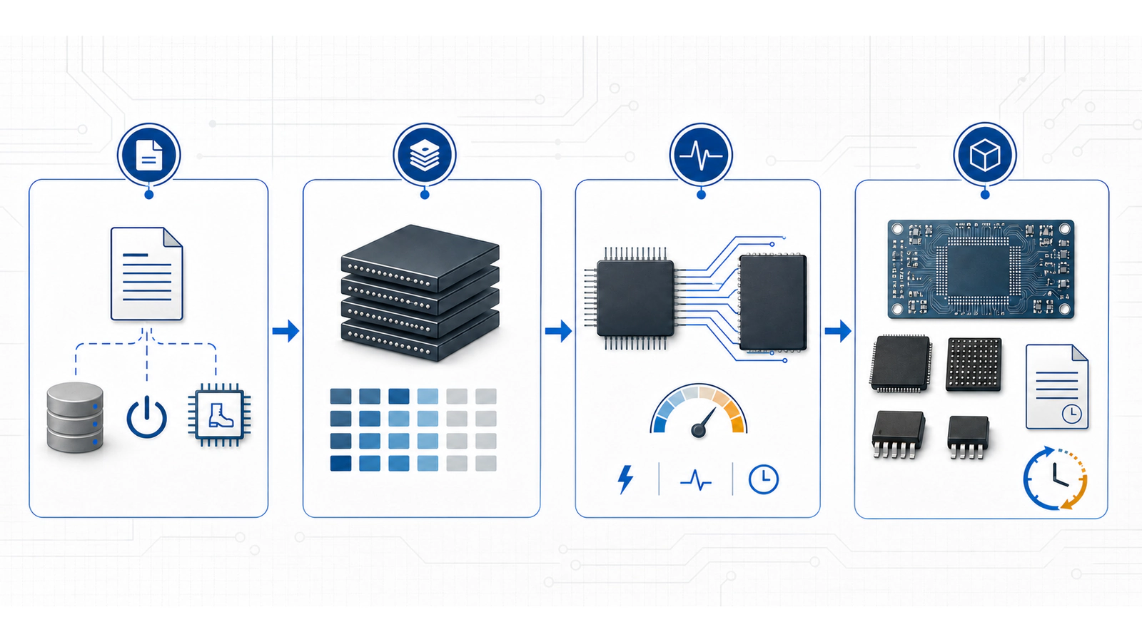
Move from the data requirement to capacity, electrical and interface fit, then package and lifecycle review.
Add reliability, temperature, qualification, security, and lifecycle gates
Before approval, check the operating environment, data-life requirement, qualification boundary, product lifecycle, and sourcing evidence. A technically plausible Memory IC can still fail one of these gates.
Endurance, retention, and data integrity
For nonvolatile memory, compare endurance and retention under the conditions stated in the exact datasheet. Temperature, cycling, access pattern, time, and data-management method can affect the applicable limit. Translate the workload into writes per location or erase unit, expected service years, duty cycle, and worst-case temperature. Then confirm whether wear leveling, refresh, redundancy, or error correction belongs in the device, controller, or system software.
For NAND-based devices, review the required ECC and bad-block or media-management method. For DRAM and other volatile memories, review refresh, error detection or correction, and the host's supported reliability features. Do not assume that "ECC" has the same coverage, reporting, or system behavior across products.
Temperature, qualification, compliance, and security
Select the temperature grade from the real operating and storage environment, including startup, enclosure, self-heating, and any derating policy. If the product requires automotive, industrial, medical, aerospace, functional-safety, or another controlled qualification, confirm the exact orderable device and supporting evidence. A family-level claim does not prove that every density, package, or speed option carries the same qualification.
Security features also need system review. Check protection regions, one-time-programmable areas, authentication, secure boot support, unique IDs, erase behavior, debug paths, and failure recovery only when the exact device and host support them. Do not treat a security feature name as a complete threat model.
Lifecycle and sourcing evidence
Check lifecycle status for the full orderable part, not only the family. Use the current manufacturer page and dated product-change or discontinuance notices, and record when the evidence was reviewed. NTCHIP's guide to checking electronic component lifecycle status provides a repeatable evidence log. Micron's product lifecycle solutions also show how application life and requalification cost can influence a memory choice.
For a long-life or high-risk product, review:
active, NRND, last-time-buy, discontinued, or other manufacturer-defined status;
notice dates, affected ordering codes, and any manufacturer-named successor;
approved source and whether authorization is required by the project;
date-code, lot, packing, storage, and traceability requirements;
documentation, inspection, and test scope agreed before purchase;
alternate policy and the engineering owner for approval.
Use NTCHIP's quality control page and incoming inspection checklist as starting points for the sourcing discussion. The specific documentation, inspection, and testing scope still needs agreement for the part, lot, application, and RFQ. No single document or inspection result proves universal authenticity or suitability.
Use a repeatable Memory IC selection workflow
Run selection as a controlled handoff between system engineering, hardware, firmware, PCB, manufacturing, quality, and procurement. The output should be an approved orderable part or a bounded specification, not a family name with missing suffixes.
1. Write the application requirement
Define the stored data, volatility, access pattern, read/write duty, boot role, usable capacity, performance target, power states, temperature, service life, qualification, security, and failure response. Separate mandatory requirements from preferences.
2. Confirm the host boundary
Record the supported memory controllers, bus widths, protocol revisions, boot options, voltage banks, available pins, reference designs, and software stack. Identify which limitations are fixed and which can change.
3. Choose a memory family
Use the data behavior and host boundary to choose EEPROM, NOR, NAND or managed NAND, SRAM, DRAM/LPDRAM, or a specialist memory. Reject technologies that require an unsupported controller, exceed the write pattern, or fail the nonvolatile/volatile requirement.
4. Build an exact-part comparison matrix
| Requirement | Required value or condition | Candidate A | Candidate B | Evidence and owner |
|---|
| Memory type and data role | | | | System / firmware |
| Usable density and organization | | | | System / firmware |
| Interface, commands, and timing | | | | Hardware / firmware |
| Supply, I/O voltage, and power | | | | Hardware / power |
| Package, pinout, and footprint | | | | PCB / manufacturing |
| Endurance, retention, and ECC | | | | System / quality |
| Temperature and qualification | | | | Quality / compliance |
| Lifecycle and approved source | | | | Procurement / engineering |
| Documentation and inspection | | | | Quality / procurement |
Every candidate column should contain a full manufacturer part number and a source document revision or URL. Mark unknowns instead of copying a family-level value into an exact-part row.
5. Review schematic, PCB, and software impact
Check the pinout, voltage domains, clocks, resets, pull-ups, decoupling, termination, routing, footprint, boot configuration, driver, memory map, update process, diagnostics, and manufacturing test. A candidate that requires changes should enter the change-control process before sourcing approval.
6. Plan verification for the real risk
Define prototype, bench, environmental, power-cycle, update/recovery, endurance, performance, and production tests that apply to the application. The manufacturer datasheet sets component limits; the product team must still verify the device inside its own hardware and software.
7. Approve the MPN and alternate policy
Release the complete orderable MPN, accepted package and grade, approved sources, and any qualified alternates. State whether alternates are prohibited, pre-approved, or subject to engineering review.
8. Release sourcing data under revision control
Add the approved part and evidence to the BOM or approved-parts record. NTCHIP's guide to preparing a BOM for RFQ shows how to keep identifiers, quantities, alternates, lifecycle flags, and documentation requirements visible to suppliers.
Prepare a quote-ready Memory IC RFQ
An RFQ should identify either an exact approved part or a clearly bounded engineering requirement. Do not send only "16 MB SPI memory" or a short top marking. The supplier should not have to infer the manufacturer, package, voltage, speed, grade, or alternate policy.
| RFQ field | What to provide |
|---|
| Original manufacturer | Manufacturer shown in the approved engineering record |
| Full manufacturer part number | Complete orderable MPN with all meaningful suffixes |
| Memory type and role | EEPROM, NOR, NAND/managed NAND, SRAM, DRAM/LPDRAM, or other; include boot, code, configuration, buffer, or storage role when useful |
| Density and organization | Raw or usable capacity requirement, data width, organization, and any page/block/bank constraint |
| Interface and speed | Protocol or bus generation, I/O width, clock/access requirement, and host/controller reference |
| Voltage and power | Supply and I/O ranges, power mode, and any sequencing constraint that affects the choice |
| Package and packing | Exact package code, footprint constraint, temperature/qualification grade, and tape/reel, tray, tube, or other packing need |
| Quantity and schedule | Prototype, immediate, production, or forecast quantity plus target date and destination |
| Lifecycle and alternate policy | Exact-only, approved alternates, engineering-review required, and any status or longevity requirement |
| Quality and documentation | Date/lot requirements, traceability expectations, compliance documents, inspection, test, or customer-specific acceptance criteria |
| Supporting evidence | Current datasheet, schematic requirement, approved-parts record, or comparison matrix when needed to resolve ambiguity |
If the exact part is already approved, send the full MPN and state that substitutions require written engineering approval. If the design is still open, label the request as a sourcing review and identify every non-negotiable requirement.
Request a quote from NTCHIP with the manufacturer, full part number, quantity, target date, and any package, lifecycle, documentation, or quality requirements. Availability, pricing, lead time, documentation, and inspection scope should be confirmed through the RFQ for the exact requirement.
Memory IC selection FAQ
Can I use a larger-density Memory IC?
Only after engineering review. A larger device may need extra address bits, different commands, a new memory map, larger erase units, more boot time, different power behavior, or firmware changes. The package and pinout may also differ. Compare the exact datasheets and validate the host, PCB, software, update, and test impact.
Are two SPI flash devices interchangeable?
Not by interface name alone. SPI devices can differ in voltage, mode, commands, status registers, identification, address length, dummy cycles, erase geometry, protection, reset behavior, maximum clock, package, pinout, and boot-ROM or driver support. Treat any alternate as a datasheet and system comparison.
What does a voltage suffix in a Memory IC part number mean?
Its meaning is manufacturer- and family-specific. It may identify a supply option, I/O voltage, speed, temperature, package, revision, or another orderable attribute. Use the current manufacturer ordering table and full datasheet. Do not decode a suffix by analogy with another family.
Does the same BGA size mean the same pinout?
No. Equal body dimensions and ball pitch do not establish the same ball map, signal assignment, data width, power pins, or no-connect rules. Compare the package drawing, ball table, recommended land pattern, and complete ordering code.
How much density headroom should I add?
Use a requirement-based margin. Include update and rollback images, metadata, logs, worst-case record growth, reserved or managed areas, and planned features. An arbitrary percentage can be too small for a dual-image update or wasteful for a fixed configuration store. Document the reason for the margin and verify usable rather than nominal capacity.
Which fields are essential for a Memory IC RFQ?
Provide the original manufacturer, complete MPN, quantity, target date, memory type, density and organization, interface and speed, supply and I/O voltage, exact package and grade, alternate policy, lifecycle requirement, and any documentation or inspection conditions. If the MPN is not fixed, identify which fields are mandatory and who approves a proposed candidate.
Can procurement approve a substitute from density, interface, voltage, and package alone?
No. Those fields are a useful screen, but engineering still needs to compare timing, commands, organization, pinout, power-up behavior, firmware and boot support, endurance or refresh, temperature, qualification, security, lifecycle, and validation requirements.
Conclusion
A sound Memory IC choice starts with the data and host, then narrows candidates by memory type, usable density and organization, complete interface behavior, voltage and timing, and the exact package. Reliability, temperature, qualification, security, lifecycle, and sourcing evidence decide whether the candidate is ready for approval.
For sourcing review, send NTCHIP the full manufacturer part number or the approved specification, required quantity, target date, alternate policy, and quality or documentation requirements. Use the Memory IC RFQ form to confirm available options, pricing, and lead time for the exact request.